Optical metamaterials are truly revolutionary: their properties (for example, a printable negative-index material) are like no other, and their nanoscale structure can be varied as a function of position to create unusual devices -- such as "cloaks." The idea is that the electromagnetic properties within the cloak create a coordinate-transformed space that can divide and channel light around an object and recombine it to form a seemingly undisturbed wavefront. Great idea, and extremely difficult to achieve, especially for objects larger than a few wavelengths in size.
It's also extremely difficult to write about, especially by the general press -- which incessantly mangles the topic by prattling on about Harry Potter invisibility cloaks, making readers or viewers think that Harry Potter-style magic is just around the corner.
By the way, in the above example, the "invisibility cloak" is not a metamaterial cloaking device at all. It's simply a switchable photothermal mirror. (Note to the general press: my bathroom mirror is not an invisibility cloak, either.)
So where does the uninformed reader, who is even less informed after reading pop-sci Potter-material articles, expect the first consumer-grade invisibility cloak to appear?
Hammacher-Schlemmer -- where it is simply called "The Invisibility Cloak."
The Apple Store -- where it comes in the form of an iPhone skin.
A toolbar for your browser -- without the feature, the toolbar is gray; with it, the toolbar is gray.
Military surplus -- yeah, we all know the feds developed this years ago and are walking among us even as we speak.
Laser Focus World -- actually, no, you won't find it here. Sorry.
Ah, who can forget the 2010 50th anniversary celebration of the laser? Our normally docile and academic-minded photonics industry was jumping in 2010, with jubilant celebrations of Lasers in the City of Lights, a special Laser Focus World Photonic Frontiers issue celebrating 50 Years of Lasers, and even an awesome "LasersRock!" festival at CLEO 2010.
Everyone loves a celebration, and I must say I was sad to see the laser anniversary end. Fortunately, many photonics inventions and companies sprang from the invention of the laser, and 2011 continues the celebration with a number of memorable 50-year anniversaries:
50 years of nonlinear optics
At the 2011 Stanford Photonics Research Center (SPRC) Annual Symposium, attendees were treated to several special sessions highlighting 50 years of nonlinear optics. Nonlinear optics veterans Chris Ebbers and Bob Byer gave a historical perspective on the National Ignition Facility and Stanford's demonstration of the first tunable CW parametric laser via optical parametric oscillation (OPO), respectively.
50 years of Spectra-Physics
While it is not extraordinary for a technology to see a 50th anniversary, it is a much rarer event for a photonics company to see such a milestone. But just this year, Spectra-Physics, now a Newport Corporation Brand, turned 50! And on the evening of September 8th, 2011, about 180 people gathered in Mountain View, CA to celebrate the golden anniversary of the first commercial laser company. Spectra-Physics was founded by five former Varian employees and incorporated on September 8, 1961--exactly 50 years earlier.
IMAGE: The Spectra-Physics 50th Anniversary celebration drew attendees from across the laser industry and beyond. (Courtesy Newport Spectra-Physics)
All three surviving founders, Arnold Bloom, Herbert Dwight and Kenneth Ruddock were in attendance at the event.
IMAGE: Herb Dwight (left) and Ken Ruddock (right), two of the founders of Spectra-Physics, celebrate its 50th anniversary. (Courtesy Newport Spectra-Physics)
The large crowd, consisting, mostly of former employees, included 6 of the first 13, as well as many former executives and division managers of the firm. The founders and guests shared vintage photos, stories from the birth of the laser industry, and had a great evening all around. The celebration was held not far from the block in Mountain View where Spectra-Physics laser operations were centered, producing a stream of laser industry “firsts” for about 48 years.
IMAGE: Attendees sign a 50-year timeline documenting their arrival at Spectra-Physics. (Courtesy Newport Spectra-Physics)
And in 2012: 50 years of diode lasers
But wait, the celebration continues into 2012, which is the official 50th anniversary of the diode laser--those little solid-state beacons of light that have found their way into our lives in countless ways.
At the 2012 Lasers & Photonics Marketplace Seminar, held during Photonics West 2012 on Monday, January 23rd (and in my shameless plug, the ONLY event anywhere in the world that focuses on the entire laser marketplace), David Welch, executive VP and chief strategy officer of Infinera, will present "Celebrating 50 Years of Laser Diodes." Believe it or not, lasing in semiconductor diodes was first observed in 1962--two short years after the first demonstration of the laser. Join Welch at the seminar as he talks about the evolution of the diode laser business, and help Laser Focus World celebrate the numerous opportunities that the diode laser has brought to all of us in the photonics community.
The commoditization of high-tech builds on itself. For example, CMOS imagers are used in digital cameras, become cheaper to manufacture, and are used in cell phones and toys. In the process they become even lower in cost, smaller, sturdier, and easier to use.
In one example that will likely continue this trend, Jonas Pfeil, who recently graduated from the Technical University of Berlin, took 36 of these imagers and created a portable, rugged camera that takes a spherical panoramic shot of its surroundings. To use it, you just toss the ball-shaped imager into the air: its internal accelerometer (another commoditized device) and some integration software predict the ball’s highest point and snap simultaneous pictures from all its CMOS imagers. The info is then downloaded via USB and viewed in custom-written spherical-panoramic viewer software.
(Image: Jonas Pfeil, http://jonaspfeil.de/ballcamera)
The project was Pfeil's diploma thesis. He and his colleagues at TU Berlin will be presenting the camera as the Emerging Technologies demonstration 'Throwable Panoramic Ball Camera' at SIGGRAPH Asia 2011 (Hong Kong; Dec. 12 to 15).
The 2-megapixel cell-phone-camera modules are held in a structure fabricated by a 3D printer, which also holds a layer of foam padding. When thrown, the device can capture scenes with many moving objects without ghosting. The inventors are currently looking for an investor or a partner to build the camera.
I can see many potential uses for this ball camera. A tourist gets a panorama of the Grand Canyon. A tweener gets a shot of all her partying BFFs at once, even the ones sneaking vodka. An undersea scientist gets accurate counts of fish and other sea life. A CIA agent gets that essential bit of info from outside a second-story window. And (with video rather than still images), an IMAX theaterful of viewers gets motion sickness.
I personally have an Android phone instead of an iPhone. Since Android is actually more popular than iOS for phones, I've been waiting for more Android photonics apps and such to appear (there are some already, such as a fluorochrome search app from Chroma Technology).
Yesterday, John Canning of the University of Sydney let me know that the use of Android devices as photonics hardware is advancing, as illustrated by an experiment in which he and his colleagues use an Android smartphone (the HTC Desire) as the light source for a fluorescence-microscope setup.1 The blue light is from the phone's OLED screen, and a freely downloadable color-flashlight app from the Android market is the spectral control.
Specimen under Android phone illumination: (a) white light (RGB); (b) blue; and (c) excited by blue and filtered to pass only fluorescence. (Images: University of Sydney)
The specimen is placed on a slide directly atop the OLED screen; the blue emission, which peaks at 445 nm, excites the fluorone dye Rhodamine 123 inside a silica mesostructure sphere. A green filter passes only the resulting fluorescence to the microscope optics. The researchers believe that a custom app would raise the signal intensity and allow rapid modulation for fluorescence-decay measurements. In addition, modifying the setup to use the phone's own camera will further simplify the device raising its potential for use in remote areas.
The authors point out that a big advantage of Android is its open access, which allows total software control, making it straightforward to integrate the phone with other hardware.
REFERENCE:
1. John Canning et al., Sensors, 11, p. 7055, 6 July 2011; doi:10.3390/s110707055.
If you're able to attend the 2011 Frontiers in Optics conference (FiO 2011; www.frontiersinoptics.com)--the OSA's 95th Annual Meeting that also includes the Laser Science XXVII conference--there are several special events and significant research papers that should not be missed. To be held next week from October 16-20 in San Jose, CA, the annual conference focuses on the timeliest research and development topics in optical science and engineering, with eight conference tracks, FiO 1 through FiO 8, on Optical Design and Instrumentation, Optical Sciences, Optics in Biology and Medicine, Optics in Information Science, Fiber Optics and Optical Communications, Integrated Photonics, Quantum Electronics, and Vision and Color, respectively.
To find out what's hot in each of the eight conference tracks, the Sunday night (4-6 pm in the Fairmont Regency Ballroom) "What's Hot in Optics Today" special event is a good place to start. Here, the Division chairs of OSA's technical groups will present overviews of recent developments in various subfields of optics in an informative and accessible manner. And hopefully you'll attend the Sunday evening welcome reception that immediately follows from 6-7:30 pm in the Sainte Claire Hotel Ballroom.
Beginning Monday, October 17 at 4:45 pm in paper FMI3, Cornell researchers present "Demonstration of Temporal Cloaking," showing for the first time how an event in the time domain can be cloaked using time-space duality concepts and novel split time-lenses.
On Wednesday, October 19 at 11:45 am, don't miss paper FLW4 entitled "Controlled Synthesis of Gold Nanorods and Application to Brain Tumor Delineation" in which a Duke University research team explains how they are using gold nanorods for tumor delineation due to their unique optical properties and biocompatibility; the nanorods effectively label tumors within brain slices.
And just after that during Wednesday's poster session from 12-1:30 pm, a team from UC Davis presents poster JWA8, "Microscopy and Spectroscopy on a Cell Phone." Laser Focus World has been covering cell-phone-based photonics for a while now, but the applications (no pun intended; is there an app for that?) continue to grow.
IMAGE: From left to right, blood-cell images showing normal, iron deficiency anemia, and sickle cell anemia types of blood are compared when using a traditional microscope (upper) and the iPhone microscope (lower). The iPhone details are clearly adequate enough to distinguish between the three blood samples. (Courtesy UC Davis)
And although this video is a few years old, Aydogan Ozcan from UCLA explains in simple terms the benefit of cell-phone microscopy:
There is also another good video from UC Berkeley on their CellScope at http://youtu.be/5qcJySNLs84.
Moving right along (it's easy to get caught up in this "smart" phone world) … don't miss the Wednesday afternoon presentation at 4 pm (paper FWW1) entitled "Bio-Inspired Photonic Nanostructures and Lasers" to see how Yale University physicists are creating biomimetic-based photonic nanostructures that confine light, leading to efficient lasing that is tuned via structural parameters.
In addition to the Monday morning (8-noon) Plenary session in the Fairmont Regency Ballroom, the exhibit hall will be open on Tuesday, October 18 from 10-4 pm, and Wednesday, October 19 from 10-2 pm. So far, a total of 80 exhibitors will be available to actually show how ground-breaking research is being translated into helpful research tools and useful, everyday products.
Laser Focus World chief editor Conard Holton and I will be attending the show off and on from Sunday through Thursday; please email me at gailo@pennwell.com if you have some interesting FiO-related research or product development news to share with us either before, during, or after the conference. See you there!
First, the science (I'll go through this quickly, because I want to get to the art). Optical contacting is a method of adhering two pieces of polished glass together without using cement. It takes advantage of very short-range molecular attraction; as a result, the two cleaned surfaces have to have exactly the same shape down to a couple of nanometers. Usually, both surfaces are flat, but can in certain instances be convex/concave. Because the surfaces are in contact, their glass/air interfaces essentially disappear and there is no Fresnel reflection whatsoever. Optical contacting is an excellent way of assembling certain ultraprecise optical components and systems, and has other uses in the optical shop as well.
Back when I was an optical engineer, I worked with some very talented optical technicians who made this technique seem easy. Then for fun I tried it -- and could never get it right. I saw splotches of rainbow colors, which were interference fringes where the surfaces did not bond; I saw little circular reflective areas where some specks of dust remained, preventing the contacting from happening. NASA should be very happy that I'm not on their team.
Art that needs excellent scratch/dig specs
Now, on to the art. I recently visited LightMachinery (Nepean, Ontario), which, along with excimer and CO2 lasers, makes precision optics. As I was leaving, Vaz, one of the company's optical technicians, handed me a document, which I looked at later in the day. As it turns out, Vaz Zastera is an expert at optical contacting, not only for LightMachinery but for his own art too.
For his optically contacted art, he works in collaboration with another artist named Jiri Harcuba. Jiri will do an engraving on an ultraflat piece of glass that Vaz has made; Vaz then optically contacts the piece to another flat, creating a larger glass object within which the engraving floats. Vaz also creates optically contacted art pieces that are unengraved.
Optically contacted three-layer sandwich; engravings in each layer inside by Jiri Harcuba. Cold work by Vaz. (Courtesy of Vaz Zastera)
Optical contacting technique was used to assemble "Dove." Eight dove prisms are optically contacted to a big right-angle prism. (Courtesy of Vaz Zastera)
And now for some science: This is an optical assembly for a first-of-its-kind instrument for Boston University and NASA. It is called a Monolithic Achromatic Nulling Interference Coronagraph (MANIC). It will be used in a telescope system to block (null) out suns when observing exoplanets (planets orbiting a star other than our Sun). It is all optically contacted. (Courtesy of Vaz Zastera)
By the way, Vaz's site says, "Optical contacting can be easily learned with practice." Hah. Maybe if you’re not a fumblefingers like me.
Back in early August, the National Aeronautics and Space Administration (NASA; Washington, DC) announced its "Can you see it now?" campaign in which the Innovative Partnerships Program Office (IPPO) at NASA decided to license the wavefront sensing and adaptive optics technologies, procedures, and lab equipment from the James Webb Space Telescope program to private industry.
But in addition to those wavefront sensing and adaptive optics technologies, the IPPO office at NASA Goddard Space Flight Center (GSFC; Greenbelt, MD) is also licensing their hierarchical image segmentation (HSEG) algorithm. This HSEG technique--originally developed for Earth science image enhancement and analysis more than a decade ago--is entering a new frontier in the medical imaging market as a powerful diagnostic tool, thanks to the licensing program.
NASA Goddard says that when Dr. James Tilton started development of his HSEG algorithm, he gave little thought to its possible medical applications. However, a workshop sponsored by Goddard’s IPPO brought HSEG to the attention of an entrepreneur in the medical imaging market and helped launch a product with the potential of saving a significant number of lives.
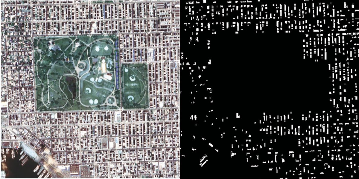
The HSEG algorithm closely intertwines image segmentation via region growing, which finds spatially connected region objects with region object classification and then groups those sets of region objects together into region classes. This feature of HSEG provides the potential of using spatial pattern recognition to recognize land use categories. As an example, consider a portion of a satellite image depicting the Patterson Park area of Baltimore, MD:
IMAGE: In one example, the hierarchical image segmentation (HSEG) algorithm uses spatial pattern recognition to recognize land use categories. (Courtesy NASA Goddard)
The HSEG analysis of this image shows a certain regularity of the roof pattern to the southeast, east, and north of Patterson Park indicative of an older residential area. The roof pattern to the southwest and west of Patterson Park has a denser concentration of businesses and apartment complexes. Pixel-based analysis could never detect this difference in spatial patterning.
So how did the life-saving medical application come about? About ten years ago, the GSFC IPPO hosted a workshop to showcase its technologies for the business community. In attendance, Fitz Walker, president and CEO of a small company called Bartron Medical Imaging (Largo, MD), saw immediate potential for HSEG as a diagnostic tool that could be adapted to enhance medical imagery, allowing for quicker and more accurate identification of problematic tissues such as cancer. Bartron licensed the technology from Goddard, which is now FDA-approved as MED-SEG, a tool that helps clinical professionals interpret medical images.
IMAGE: An original mammogram is shown before MED-SEG processing (left), and after MED-SEG processing (right), indicating a region of interest in white. (Courtesy Bartron Medical Imaging)
The Bartron website says that MED-SEG provides improved diagnoses for a wide range of medical images, including CT and PET scans, MRI, ultrasound, X-ray, digitized mammography, soft tissue analysis, and moving object analysis including microscopy and endoscopic examinations. Physicians and health care practitioners can take any unmanipulated medical image and segment it to ‘see’ features in the image that were not previously visible to the naked eye, isolating one particular area of interest in an image to compare it with many other reference images databased at other health care facilities, for instance. Bartron says the MED-SEG system brings out properties not seen with the naked eye or with current imaging enhancement systems.
NASA Goddard wants to remind the photonics community that it continues to develop HSEG for licensing opportunities in markets as diverse as facial recognition, image data mining, and crop monitoring. If you have a new frontier in mind for such a technology, please contact the GSFC IPPO at http://ipp.gsfc.nasa.gov/index.shtm. Who knows, space may not be the “final frontier” after all!