Monday, December 10, 2012

Holmium for the holidays


Chemical elements are the gifts that keep on giving. This holiday season, it's important to acknowledge how much the chemical elements--and especially the rare-earth elements--keep our photonics industry humming. As I prepare to write my February Photonics Applied feature article on "Photonics Materials", I am reminded of how precious these chemical elements are to the livelihood of our industry and unfortunately, how precarious their supply really is.

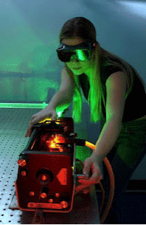
For example, take the lanthanide and rare-earth element holmium (Ho), atomic number 67. According to Wikipedia and the Royal Society of chemistry's online periodic table (www.rsc.org/periodic-table), holmium and all the other rare-earth elements including cerium (Ce), neodymium (Nd), erbium (Er), thulium (Tm), and ytterbium (Yb) share something in common: they are at "high risk" in terms of supply. Like many of the rare-earths, holmium rarely occurs in pure form in nature. A soft and malleable silver-white metal (see image), it is extracted from other metallic minerals using caustic and acidic processes. Holmium oxidizes rapidly into several forms of holmium oxide. While benign in its elemental form, many of the isotopes of holmium are radioactive.

Although abundant in nature at 1.3 mg/kg of earth (more than 20 times more abundant than silver according to www.lenntech.com/periodic/elements/ho.htm), the environmentally unhealthy separation process means that nearly 97% of the supply comes from China. A recent Forbes article (www.forbes.com/sites/jackperkowski/2012/06/21/behind-chinas-rare-earth-controversy/) highlighted the
controversy, in which China published its first white paper and indicated that it had a smaller percentage (23% of the world's supply) compared to the 36% it was estimated to have. The report raised stock prices for non-Chinese mining companies and recent quotas on exports from China are alarming rare-earth purchasers. Indeed, other nations have simply stopped mining the stuff (see chart).


Because holmium has the highest magnetic moment of any of the rare-earths, it possesses unique properties that make it useful in building ultrastrong magnets, in absorbing nuclear-fission-created neutrons, and as a dopant material in solid-state and fiber lasers. In fact, holmium YAG lasers are used with much efficacy in laser-based surgical applications. For example, a video at http://youtu.be/3TDI8kmU9C0 shows how holmium lasers can remove kidney stones, and another video here shows how a holmium laser is used to treat urethral stricture--an abnormal narrowing of the tube that carries urine out of the body:


So what would the holidays be without our rare-earths? Ask any photonics company and they will tell you, not at all joyful. I'm not a fan of mining and its harmful effects on the environment, but it's clear that the geographic availability of these rare-earth elements needs to be expanded. Stay tuned for my February feature article on photonic materials and the many surprising uses for common and not-so-common chemical elements in our photonics industry. And until then, here's hoping you'll get a big Ho-Ho-Ho from Santa this holiday season!

Tuesday, November 13, 2012

Image projection via caustics -- wow!


I just came across a method for projecting a monochrome still image that is stunning in both its simplicity and efficiency. Developed at École Polytechnique Fédérale de Lausanne (EPFL; Lausanne, Switzerland), the method relies on an acrylic projection "slide" that has nothing embedded within it and nothing printed on it, but instead has a surface shaped to be slightly uneven.

Place it at the right point between a reasonably small, bright light source and a wall, and an image appears. The image is formed from the "caustics" that arise when an optically smooth but rippled surface slightly and unevenly deflects light, producing lighter and darker areas (such as what you see at the bottom of a swimming pool on a sunny day).

Form the ripples in the right way, and you can project whatever image you want -- such as this image of Alan Turing, the British mathematician and father of modern computer science, shown in the light of an ordinary white LED.

Credit: (c) Alain Herzog

The surface shape to provide a specific image is calculated via an algorithm. Because this type of projection doesn't rely on absorption, the process is virtually lossless. Almost any transparent item could be made into a projector -- windows, display cases, architectural ornamentation, vases, glasses, jewelry, and so on.  See this EPFL Youtube video for more.


Researchers in EPFL's Computer Graphics and Geometry Laboratory showed working image-projecting caustic plates recently at the Advances in Architectural Geometry Conference in Paris. Contributors to the project include Mark Pauly (EPFL), Thomas Kiser (EPFL), Michael Eigensatz (Evolute; Perchtoldsdorf, Austria ), Minh Man Nguyen (WAO Architecture; Paris, France) and architect Philippe Bompas.

Thursday, November 8, 2012

Telepresence to go microscopic?

A couple of weeks ago (on Halloween, in fact), I posted a news story to Laser Focus World about "telepresence" robots crafted especially to allow people to attend corporate meetings; the remote attendees wear head-mounted displays and other devices, while at the other end their physical robot avatars sit at the meeting, displaying facial expressions and waving their hands impatiently.

However, this is only the beginning. A group of European and American scientists recently created a somewhat similar telepresence system, except that the meeting consisted of one human and one rat.1 The human, who wore an eye-tracking head-mounted display, was represented by a rodent-sized robot that allowed the person to communicate with the rat on its own scale; the rat, tracked by two stereoscopic cameras, was represented to the human as a humanoid avatar on a computer screen. The human got to play carefully scripted games with the rat; the rat got to play along and occasionally receive a dab of jam for a reward.


So what's next? Well, back in the 1960s, a science-fiction movie, Fantastic Voyage, was based on the implausible idea of shrinking a submarine and a few people to microscopic size and injecting the sub into someone's body so that the crew could find and eliminate a blood clot. It made little sense then, but telepresence could make this sort of thing a reality (minus the teeny humans).

For example, the "Pillcam," invented by Given Imaging (Yoqneam, Israel) more than ten years ago and now moving toward FDA approval, is swallowed by a patient and moves naturally through the patient's gastrointestinal tract looking for polyps, conceivably eliminating the need for a colonoscopy. Such devices could be made smaller -- perhaps much smaller -- and could possibly be steered or even self-propelled, delivering drugs or doing microsurgery. As for photonics hardware, an extreme version of a camera-on-a-chip would be needed for vision, and other (perhaps plasmonic) sensors would be a must. Or the devices could be tracked using optical coherence tomography (OCT). Or . . .

Rats, I have to get back to work.

REFERENCE:

1. Jean-Marie Normand et al., PLOS ONE (2012) doi:10.1371/journal.pone.0048331.


Tuesday, October 30, 2012

Industry leaders to speak at Laser Marketplace Seminar


A host of industry leaders will help us celebrate the 25th anniversary of the Lasers & Photonics Marketplace Seminar on Monday, February 4, during SPIE Photonics West in San Francisco. The keynote speaker is Valentin Gapontsev, chairman and CEO of IPG Photonics, who will discuss developments in and opportunities for the fastest growing laser segment--fiber lasers.

There will also be great talks on market and technology trends by leaders such as Eric Swanson from OCT News on developments in optical coherence tomography, consultant Bo Gu on laser markets in China, Rüdiger Paschotta from RP Photonics on optical components for ultrafast lasers, and Parviz Tayebati from TeraDiode on high-brightness, direct diode lasers. In addition, Petros Kotidis from Block Engineering will talk about opportunities for quantum cascade lasers and Wilhelm Kaenders from Toptica will describe emerging applications for supercontinuum lasers.

To provide data and forecasts about sales of lasers, Allen Nogee, senior analyst at Strategies Unlimited, and David Belforte, editor in chief of Industrial Laser Solutions, will provide in-depth analyses of global laser markets.

The audience will also learn about recent trends in mergers and acquisitions from Robert Mandra at RSM Advisors, and hear about a rapidly developing model for taking advantage of IP and techology innovations from Jason Eichenholz at Open Photonics.

The continuous turmoil and uncertainty in the world economy has made many photonics companies cautious, even as some have done very well in specific product areas. As a result, the insights and networking you'll find at the Seminar should be of great interest--I hope to see you there.

For the Full Agenda and to register, please click HERE.


Wednesday, October 24, 2012

InterOpto takes fireflies very seriously

The September 25-27 InterOpto 2012 conference in Yokohama, Japan, was far removed from its roots as a telecom show in the years leading up to the bubble. While communications and optical components continue to be a focus for the InterOpto conference and its exhibitors, the conference has expanded to include not only InterOpto 2012 (optics and photonics), but also BioOpto Japan 2012 (biomedical optics), LaserTech 2012 (industrial lasers), and the LED JAPAN Strategies in Light (LED technology) conference. In fact, the LED JAPAN Strategies in Light conference complements the US-based Strategies in Light conference held each February in Santa Clara, CA (with 4600 attendees and 200 exhibitors) as well as the Strategies in Light Europe conference (September) and the Strategies in Light China conference (May). Strategies in light deals exclusively with LEDs and solid-state LED lighting technology. In addition to the conference programming, nearly 185 exhibit booths across the InterOpto, BioOpto, LED JAPAN, and LaserTech conferences were assembled in one area.


The LED exhibit (60 booths) included a wide range of LED and illuminance testing products from Konica Minolta (booth L-146) including their new CL-500A Illuminance Spectrophotometer--a very compact spectrophotometer for evaluation of LED lamps and electroluminescent materials. Its advanced sensor measures CRI (color rendering index), illuminance, chromaticity, and color temperature for any light source in a laboratory environment or out in the field. Who knew Konica Minolta had so many illuminance measurement products? Their portfolio includes Chroma Meters to measure color temperature,
and whole family of other illuminance meters (including integrating spheres) for any application.

Within InterOpto's new JIAL (Japan Importers Association of Lasers and Electro-Optics) Global Technology Seminar at which I presented the keynote entitled "Mid-Year 2012 Laser Market Review & Forecast", companies such as Coherent, Spectra-Physics, nLight, Oclaro, Amplitude Systemes, NKT Photonics, and Jenoptik presented overviews of their latest technology breakthroughs primarily in the laser industry. Of particular note in the spirit of the 2012 50th anniversary of the laser diode, DirectPhotonics Industries GmbH presented "Ultra-High Brightness Direct Diode Lasers for Material Processing." Fiber lasers may be seeing direct-diode competition sooner than anticipated if DirectPhotonics can leverage Fraunhofer technology to hone its single-emitter-based, wavelength-stabilized, spectrally combined system into a 2 kW, 7.5 mm mrad beam profile at 9xx nm into a production-ready machine. Its current DirectPump 900 source offers 90 to 600W for pumping applications, with more products being added to their portfolio.


The InterOpto exhibit was 84 booths strong, with many US-based as well as Japanese companies represented. With smaller exhibitions, LaserTech 2012 (16 booths) and more specifically, BioOpto Japan 2012 (21 booths) featured some excellent seminars. BioOpto Japan included Shinoda Plasma's presentation on a Luminous Array Film technology for a deep-ultraviolet light source, Furukawa Electric's description of its live-cell, damage-free cell flow cytometer, Nippon Dental University's presentation on dental caries prevention with a low-power laser, and Tokyo General Hospital discussed the role of low-level light therapy (LLLT) for the treatment of pain. And on the environmental front, Shojiro A. Maki from
the University of Electro-Communications presented his work on NIR probes based on firefly luminescence--the ultimate biomimetics success story in harnessing nature's best for the photonics industry.

As I took some time to vacation in Tokyo and Yokohama and visit some of the fine-art galleries, I was reminded of Japan's close tie with the natural world. And back at the conference center, I was extremely pleased to see that Japan is making strong efforts to improve the environment with the longest line of recycling containers I've ever seen! The United States should take note in its future photonics conference
venues--just because we have more land for garbage dumps doesn't mean we need to use it for that; how about creating a firefly habitat instead?

Wednesday, September 19, 2012

Laser update keynotes InterOpto JIAL Seminar

At this year's InterOpto 2012 conference in Yokohama, Japan, Laser Focus World will present a mid-year laser market update and outlook (www.optojapan.jp/interopto/en/jial_seminar.html) as we prepare for the 2013 Annual Laser Market Review & Forecast to be published in the January 2013 issue of Laser Focus World magazine. The full 2012 Worldwide Market for Lasers report is available now through Strategies Unlimited (Mountain View, CA), the marketing and analysis arm of PennWell that compiles the quantitative data for our annual laser market review.


I was honored to be asked to keynote the new JIAL (Japan Importers Association of Lasers and Electro-Optics) Global Technology Seminar at InterOpto--a three-day event (September 25-27) with focused presentations on industrial laser materials processing (see David Belforte's mid-year industrial lasers webcast), ultrafast lasers, supercontinuum advances, single-photon counting and fluorescence microscopy, terahertz generation, fiber coupling and microoptics, biophotonics, and even measurement of aspheric and freeform surfaces. My keynote will of course focus on the laser market itself, which is intimately tied to all things photonic-related; lasers are in fact enjoying moderate growth as a $7+ billion dollar market (), and all indications are that growth will continue to be moderate through 2015 barring any unforeseen, catastrophic events.

The JIAL Global Technology Seminar is organized by OITDA, the Optoelectronics Industry and Technology Development Association (www.oitda.or.jp), and the media sponsor is PennWell's own Laser Focus World Japan, which now has around 12,000 subscribers.


So if you want to find out how the laser markets are faring, please attend the JIAL keynote at InterOpto on September 25. If you cannot attend, please be sure to register for the Laser Marketplace Seminar (www.marketplaceseminar.com) on February 4, 2013, held in conjunction with Photonics West 2013 in San Francisco, CA. As the "aftershocks" of the economic recession continue to rumble, it will be interesting to see how 2013 plays out for our laser industry--and whether our modest forecast will be accurate.

Monday, September 17, 2012

Fruit of the laser diode


In July 1962, Robert Hall and some colleagues at the GE R&D Center in Niskayuna, NY, succeeded in doing what researchers in other labs in the US, France, Russia and elsewhere were seeking: to create coherent light emission from GaAs junctions—giving rise to the first laser diode. In September that year, Hall published the results in Physical Review Letters and the rest, as they, is history.

To celebrate the 50th anniversary of his seminal paper, you can listen to one of the leaders in more recent laser diode advances, David Welch, co-founder of Infinera, present a webcast on the past and future of laser diodes.

In the September issue of Laser Focus World, we celebrate the laser diode with an article by researchers at KMLabs and the Colorado School of Mines on using blue laser diodes to pump a Ti:sapphire laser—illustrating yet one more application for this extremely versatile tool that also enables optical data storage and fiber optic communications.

These two laser-diode-enabled optical applications, along with displays, are the reasons that companies such as Microsoft are now hiring hundreds of experienced optical engineers. This says much about current competitive markets and the powerful enabling roles that photonics play. Microsoft, Amazon, Google--with their readers and tablets, game boxes, fiber optic networks, and optics-based cloud farms—are prime examples of how far we’ve come since that time 50 years ago when a few researchers made a p-n junction semiconductor lase.

Friday, August 24, 2012

LIBS on Mars: nice plasma indeed

While everyone knows that ambient conditions on Mars are vastly different than those on Earth, it's interesting to see the practical results of this fact. For example, when laser-induced-breakdown spectroscopy (LIBS) is done on Mars, as with the ChemCam on NASA's Curiosity rover, the process unfolds differently than it does here in the great out-of-doors. The photo below shows this (but for now please put aside the fact that these images were taken of laser plasmas in a Los Alamos National Laboratory test chamber under atmospheric pressures typical of Earth and Mars). The image size is 75 x 75 mm; the target in both cases is a piece of metal. The Mars-like atmospheric pressure is about one-hundredth of the Earth-like pressure.


(Image: LANL)

And now the results, please. The ChemCam's LIBS setup has three spectrometers that work in the UV, the violet, and the visible and near-IR, respectively. The first analyzed rock, dubbed Coronation, is (or maybe by now, was) 2.7 m away from Curiosity. The resulting spectrum of 30 laser shots, seen below in squashed form (the larger version can be found at http://www.nasa.gov/mission_pages/msl/multimedia/gallery-indexEvents.html) shows many lines of metals and other elements, including carbon and hydrogen. Interestingly, the hydrogen only showed up in the first laser shot, indicating that it was only on the rock's surface. Note the sensitivity (very small peaks for titanium and manganese) as well as the fact that the x-axis scale is somewhat nonlinear.


(Image: NASA/JPL-Caltech/LANL/CNES/IRAP)

However, as I mentioned earlier, conditions are quite different here on Earth: instead of vaporizing rock, curiosity merely killed the cat.


Monday, August 20, 2012

Petawatts proliferate

Borrowing a phrase from a 2006 Laser Focus World petawatt article, it is even more true today that "petawatts proliferate." All petawatt lasers aim to deliver petawatt-power-level pulses. But to understand just why so many petawatt-class (or sub-petawatt-class) laser systems are either in operation or being developed, it's necessary to understand the petawatt pulse itself and the groundbreaking applications that are causing these laser powerhouses to proliferate. What is the petawatt pulse width, the pulse duration, the peak power level, and the frequency at which these petawatt pulses are delivered? And just what type of light-matter interaction studies and other applications make petawatt-level pulses so appealing?

In mid July, Laser Focus World reported that the National Ignition Facility (Livermore, CA) delivered 500 terawatts (0.5 petawatts or PW) to its target in a step towards laser-initiated fusion. The 1.85 MJ energy is generated by NIF's 192 laser beams in a football-field-sized structure. And just a month prior, we reported on Ohio State University's Science Center for Advanced Research on Lasers and Engineered Targets (SCARLET), which aims to deliver the same 0.5 PW power-level pulses from a much smaller facility with a one-shot-per-minute repetition rate (see image below). However, compared to NIF, the 30 fs pulsewidth SCARLET creates sub-millijoule pulses that have a lot of power, but cannot compare to NIF's 1.85 MJ peak.


At the extreme of the petawatt-class-laser craze is definitely the Extreme Light Infrastructure (ELI)--Europe's project that will increase the peak power of ultrashort-pulse lasers to a whopping 200 PW and peak intensities of 10exp25 Watts per square centimeter. Not yet built, the ELI will begin with a more modest 10 PW laser and advance to 200 PW by 2017. In his Photonics Frontiers article in Laser Focus World in January 2011, Jeff Hecht described some of the applications that make ELI and all petawatt-class lasers so exciting; for example, proton acceleration to the 70-250 MeV range is needed for cancer therapy and ultrahigh-energy ultrashort pulses enable photonuclear physics studies that could lead to nuclear waste disposal.

This year's OSA CLEO conference included a special Petawatt Lasers Technologies (CMD4) series of sessions, which detailed the following petawatt-class laser systems (a reference paper is linked for each):

CAEP China:
http://www.opticsinfobase.org/view_article.cfm?gotourl=http%3A%2F%2Fwww%2Eopticsinfobase%2Eorg%2FDirectPDFAccess%2FB6F01AC9%

APRI/GIST Korea:
http://connection.ebscohost.com/c/articles/50174408/0-1-hz-1-pw-ti-sapphire-laser-facility

LLE University of Rochester, USA:
http://www.lle.rochester.edu/omega_facility/omega_ep/

In addition to these CLEO presenters, petawatt laser systems are proliferating worldwide; here are a few more examples of systems in operation or systems planned to be built:

Texas Petawatt Laser, The University of Texas at Austin, USA:
http://texaspetawatt.ph.utexas.edu/overview.php

Hercules Petawatt Laser, University of Michigan, USA:
http://www.engin.umich.edu/research/cuos/ResearchGroups/HFS/Experimentalfacilities/HERCULESPetawattLaser.html

Z-Petawatt, Sandia National Laboratories, USA:
http://www.z-beamlet.sandia.gov/facilities/petawatt.html

Vulcan laser, Rutherford Appleton Laboratory, England:
http://www.clf.rl.ac.uk/Facilities/Vulcan/12248.aspx

XCELS, Russia:
http://www.xcels.iapras.ru/img/site-XCELS.pdf

PHELIX laser, Germany:
http://www-alt.gsi.de/informationen/wti/library/scientificreport2011/PAPERS/PNI-PP-21.pdf

One of the best YouTube videos available on the how petawatt lasers work and their many applications is from Todd Ditmire on the Texas Petawatt laser team. check it out, and I'm sure you'll see why petawatts proliferate and will continue to do so (at least until exawatt lasers arrive!).


Monday, August 6, 2012

Curiosity to Earth: the photonics have landed!

As we all know by now, the Mars Curiosity rover has landed -- congrats, NASA! I, along with millions of others, will be eagerly awaiting what Curiosity has to say.

Here is just a brief mention of some of the photonics companies and organizations that produced the lasers, sensors, and optics essential to Curiosity's misson.

One of the most important instruments carried by Curiosity is the ChemCam, originally developed by the Los Alamos National Laboratory (Los Alamos, NM); this instrument contains a laser-induced breakdown spectroscopy (LIBS) system that will spectroscopically analyze Mars' surface.

An early image taken by one of Curiosity's hazard avoidance cameras (NASA)

The spectrometers in ChemCam were produced by Ocean Optics (Dunedin, FL), while the plasma-producing Q-switched, diode-pumped solid-state laser at the heart of the instrument was developed by Thales Laser (Orsay, France). The Chemcam also contains laser diodes from 3S Photonics (Nozay, France).

Curiosity contains 17 cameras; some of these were developed by Malin Space Science Systems (San Diego, CA), a company specializing in systems for unmanned spacecraft. CCD cameras from Truesense Imaging (Rochester, NY; a former division of Eastman Kodak) will be used for high-resolution (up to 14.4 μm per pixel) photos of rocks and other surface material, while CCD cameras from Teledyne Dalsa (Waterloo, ON, Canada) will be used for navigation and hazard avoidance.

Many of the camera optics for Curiosity were provided by Optimax (Ontario, NY).

It should also be mentioned that radiation-hardened photovoltaic cells from Emcore (Albuquerque, NM) powered the spacecraft as it headed toward Mars (the Curiosity rover itself is powered by radioisotope thermal generators).

I'd like to thank these innovative photonics outfits, along with the many that I have not mentioned here, for a job well done! And I look forward to seeing the science results that Curiosity will be producing in abundance -- along with the sweeping vistas that make many of us want to put our own footprints into the surface of Mars.


Friday, August 3, 2012

Persistent surveillance pays off


During the SPIE Defense, Security + Sensing show in Baltimore, I had a very interesting conversation with John Marion, who is director of persistent surveillance at Logos Technologies, based in Fairfax, VA. Our talk was about surveillance imaging from aerostat balloons tethered to the ground to continuously observe what Marion said could be a “small-city size area”.
Aerostats made news in May with a New York Times article describing life in Afghanistan under the eye of the many spy balloons tethered at military bases and in cities. At a relatively low cost, such balloons provide the military with an unblinking, long-term view of important areas, helping to catch insurgents planting bombs and deterring ambushes.
In 2010, General David Petraeus, commander of allied forces in Afghanistan, had asked for help from all available intelligence, surveillance, and reconnaissance (ISR) assets. In partial response, a 300-ft-long, untethered hybrid airship called LEMV (long-endurance multi-intelligence vehicle) was developed by Northrop Grumman for the US Army. Its first flight has been repeatedly delayed and now may be scheduled for November, according to one report.
To enhance the imaging capabilities of the much smaller aerostats, Logos Technologies developed its Kestrel system, which is a wide-area persistent surveillance system for forward operating bases. Its development includes novel imaging and stabilization capability for day/night operation.


To date such aerostats have relied on narrow field-of-view ball gimbal sensors to identify targets of interest. The Kestrel sensor enables 360° coverage out to extended ranges at moderate resolution, while cueing a narrow field of view camera to provide high resolution imagery of targets of interest.
The ground station system enables operators to monitor multiple regions of interest in real time, and allows for backtracking through the recorded imagery while monitoring ongoing activity (see video). This backtracking capability allows operators to detect and understand threat networks and operations. Since July, ten of the full day/night surveillance systems have been deployed to Afghanistan, with six more available as spares.


This spring the US Department of Homeland Security tested the Kestrel system for border security around Nogales, Arizona. A Raven Aerostar aerostat was fitted out with a Wescam MX-15 hi-res, narrow-field camera from L-3 Communications and a Kestrel day/night medium-res, wide-area persistent surveillance system. Thanks to the system, authorities apprehended 30 suspects on the first night of the demonstration and made a total of 80 arrests over the course of the week.


Monday, July 16, 2012

Ultrafast fiber lasers? We have a webcast for that

I am really liking the way the Laser Focus World webcast schedule is shaping up this year. We've already had many very interesting presenters, the latest being Claire Gmachl, the director of MIRTHE (the Center for Mid-InfraRed Technologies for Health and the Environment), who spoke on quantum-cascade lasers earlier this month (the webcast is still available on-demand and can be found on our homepage).

And the trend continues! Next up on July 27 is Almantas Galvanauskas, professor at the University of Michigan and cofounder of Arbor Photonics, Inc., who will be speaking on ultrafast fiber lasers. Over a period of 20 years, he has been prominent in the field of fiber lasers; he has pushed the performance of ultrafast fiber lasers to new highs and has also pioneered ultrashort-pulse fiber chirped-pulse amplification (CPA) systems.

In addition, no one can tell you better what's to come in ultrafast fiber lasers, because Dr. Galvanauskas' research is at the leading edge.

So come join us on July 27 at 1 p.m. Eastern, 10 a.m. Pacific time (the "early bird special" for this pay-per-view webcast lasts until July 20). You can sign up at http://www.laserfocusworld.com/webcasts/2012/07/ultrafast-fiber-lasers.html .

Friday, July 13, 2012

Harnessing Light study can make a difference

The release of the Harnessing Light report, due in late summer, will be an opportunity to describe to the public and policy makers the critical roles that optics and photonics play in our economy, security, and personal lives. If the companies, universities, and professional societies in the photonics community work to advance its findings, then real progress could be made in priorities such as competitive advantage, workforce needs, and manufacturing infrastructure.

As Paul McManamon, past president of SPIE and cochair of the study committee, notes in this SPIE video, the European community took note of the findings in the original 1998 report to develop its vision and policy--and has benefited ever since. More information and additional links may be found here on the SPIE website.


Wednesday, May 30, 2012

SPIE and OSA cooperate on optics education


In the April print issue of Laser Focus World, our feature article entitled "How to begin a career in photonics" erroneously stated that the Optics and Photonics Education Directory at www.opticseducation.org was from the Optical Society (OSA; Washington, DC). Unfortunately, that information was not correct (my apologies again for the error); indeed, the Optics and Photonics Education Directory--as corrected in the online version of the magazine article--is a joint public service effort by both SPIE (Bellingham, WA) and OSA. In fact, as I learned in the weeks following the release of our April issue from Krisinda Plenkovich, SPIE Education and Community Service director, SPIE actually initiated the directory back in the mid 1980s.

SPIE staff member Rich Donnelly--who still works for SPIE as SPIE Newsroom managing editor--used to get many inquiries about optics programs, so he decided to start publishing a list in the Optics in Education portion of SPIE's then tabloid Optical Engineering Reports. The first edition of the list was printed in 1985-86 and had 26 listings across North America. In 1990, the list became global and evolved into the booklet format that is used today.


But in 2001, SPIE's Education Committee and OSA's Membership & Education Services (MES) Council determined that education was one of the areas where cooperation between the two societies could benefit the entire community and the Optics Education Directory was seen as a vehicle where that cooperation could be especially productive. Consequently, it was decided at the time that SPIE would provide OSA with the content it had been using to produce a print version of the directory and OSA would utilize that information t to create an online version.

This cooperation resulted in the co-branding of the Optics and Photonics Education Directory with OSA. Today, a memorandum of understanding (MOU) exists between SPIE and OSA to define the joint collaboration and sponsorship of the Optics and Photonics Education Directory. In short, SPIE is responsible for managing the print version of the Directory--4500 copies of which were distributed in 2011 to libraries and academic institutions throughout the world (in more than 220 different countries). And OSA is responsible for updating the online version of the Directory, from which the print version content is generated. According to Kathryn Amatrudo, OSA's deputy senior director of Membership and Education, the online Directory receives thousands of visits each month.

When writing the April photonics education article, the Optics and Photonics Education Directory was indispensable for my research on just how many academic institutions exist for our students, what the entry criteria are, how large the student population is at the various institutions, what type of curriculum is offered, and of primary importance, a personal contact at the institution that is available to answer any questions students may pose. With more than 350 international listings, students considering a career in photonics have an excellent photonics education resource at their fingertips, or at the click of a mouse. Courtesy SPIE and OSA, the Optics and Photonics Education Directory is the go-to resource for aspiring photonics students and graduates of the future.


Thursday, May 10, 2012

Looking for a laser market analyst

Strategies Unlimited is seeking a senior analyst to cover the laser, LED, and photonics markets. This demanding position will be responsible for collecting data on all critical market areas, and developing market forecasts that will be published in industry reports and presented to private clients and at industry events. Familiarity with the photonics industry is highly desirable because the position requires insight into the overall global market for lasers and photonics, including market trends, supplier market shares, and market breakout by application segments and geographic regions. Strategies Unlimited is the research group of PennWell, which is the parent company of Laser Focus World. If you are interested in being considered for this position and have questions, please contact Ashley Pile in PennWell's Human Resources department: ashleyp@pennwell.com or 918-832-9357. You can find the application on our HR website.

Monday, April 16, 2012

Wearable photonics you can create and live by

Featured in our April issue of Laser Focus World is an article from Philips Research (Eindhoven, The Netherlands) entitled "WEARABLE PHOTONICS: Smart photonic textiles begin to weave their magic" that shows, among other fiber-optic and photonic-based textile styles, Black Eyed Peas singer Fergie wearing an illuminating jumpsuit.


FIGURE: Fergie of the Black Eyed Peas wows in an illuminating jumpsuit. (Courtesy Studio XO)

So what's next beyond temporary, short-lived glow-in-the-dark fashions? The evidence points to wearable photonics that illuminate for long periods of time and offer unique and one-of-a-kind design capabilities, thanks to the advent of organic light-emitting diode (OLED) and other flexible display technologies that can be woven into (or somehow incorporated) into wearable fabrics.

Case in point is a new stretchable optoelectronic panel from researchers at the University of California Los Angeles (UCLA). The stretchable polymer OLED device uses carbon nanotubes as the conductor and can be reversibly stretched by up to 50% strain without damage. The polymer light-emitting electrochemical cells (PLECs) were spin-cast on glass, laminated, and then peeled off. The blue emissive fluorene luminescent layer was sandwiched between two single-walled carbon-nanotube polymer electrodes. The sky-blue device has shape-memory capability and maintains stretchability for wearable photonic applications.

And just when you thought wearable photonics was limited to what designers hand you, how about a Lazer Shirt that lets you design your own glowing message or custom work of art?


VIDEO: How to create wearable art with the Lazer Shirt. (Courtesy Lazer Shirts)

Here is how the Lazer Shirt is described on the thinkgeek website: "Lazer Shirts are interactive white t-shirts that let you design your own creation with the power of UV light. Simply touch the ultraviolet Lazer to the shirt, press the button, and draw or write whatever you want. Step into the darkness and your shirt will glow, displaying your creative genius. When the design finally fades, you can use your UV light to draw something totally new. And even though your Lazer Shirt is magical, you can still toss it in the washing machine like every other t-shirt." The secret to Lazer Shirt is probably a UV-to-visible phosphor, although I was unable to find out exactly how it works.

Personally, I don't think I’ll be ordering a Lazer Shirt anytime soon. While fashion may be somewhat important to me, I'd rather see an increase in research activity surrounding the use of wearable photonics in soldier suits or medical monitoring applications. Embedded sensors that monitor heart rate, blood flow, and even monitor wound-healing progress while automatically (and wirelessly) reporting data back to a remote station seem like a much more admirable use of "wearable photonics". Fortunately, programs such as OFSETH, or Optical Fiber Sensors Embedded into technical Textile for Healthcare monitoring, is an EU-funded project that weaves sensors--based on Fiber Bragg gratings (FBGs), optical-time domain reflectometry, and macrobending effects--for patients undergoing magnetic resonance imaging (MRI) to monitor spontaneous respiration, which is constantly at risk of being impaired by anesthetic drugs or upper-airway obstruction.

There is also research at Eindhoven University of Technology on smart jackets for neonatal monitoring that use a combination of photonics such as reflectance pulse oximeters and embedded optical fibers. I have no doubt that these wearable photonics will save lives and improve healthcare for the next generation--photonics we can live by!

Thursday, March 29, 2012

Photonics shows strength in Shanghai

Since first opening in 2006, LASER World of Photonics China has established itself as the leading lasers and optics tradeshow in China. It was very clear to me how energized the exhibitors and attendees were by the diversity and quality of products on display, the rapidly increasing scale of the industry in China, and the international feel of the event.


The show ran from March 20-22 in Shanghai’s New International Expo Center, and attracted 475 exhibitors from 19 countries, an increase of 32 percent from 2011. The number of visitors reached 34,300, a 19 percent growth over last year. The total exhibition space increased to 23,000 sq m, up 33 percent from 2011.

Most of the major North American and European manufacturers of lasers, optics, and cameras exhibited at the show. Some were able to benefit from many years of operating subsidiaries in China; for example, Avantes China held a celebration marking its fifth anniversary and disclosed plans for growth that included expanding from four to five locations.

The vast majority of exhibitors were Chinese, including names increasingly familiar to me such as Castech, China Daheng Group, Crystech, Han’s Laser Technology, Luster LightTech, Pinnacle Scientific, Wuhan HuaGong Laser Engineering, Wuhan Raycus Fiber Laser Technologies, and Xi’an FocusLight Technologies. A section of one hall was devoted to the Machine Vision Exhibition Pavilion, which attracted approximately 100 Chinese and international exhibitors.


The Photonics Congress China was held in parallel to the tradeshow and featured the International Conference on Laser Processes and Components, the Conference on Laser Technology and Optoelectronics, an OIDA Fiber Communications Workshop, and the OSA Energy Photonics Workshop. During the Laser Processes and Components conference, I presented some of the global laser marketplace data researched by Strategies Unlimited, a summary of which was published in Laser Focus World.

The audience of approximately 300 also heard from Prof. Youliang Wang, Chinese Optical Society Laser Processing Committee, who discussed the state of the laser industry in China. The first point he made was that the central government is firmly behind the industry. The current president of China and general secretary of the Communist Party, Hu Jintao, has said, “We should redouble our efforts to research, produce, and use lasers.”

Wang also noted that two laser companies are now listed on the Shenzhen Stock Exchange (SXSE): Wuhan Golden Laser www.goldenlaser.cc (SHE: 300220) and Shenzhen Sunshine Laser and Electronics (www.sunshine-laser.com) (SHE: 300227). He said that the laser processing industry is growing quickly and embracing fiber lasers, but that much work needs to be done. According to Wang, there are 50 domestic high-power laser companies but only 13 of them are well known and have a strong intellectual property position and R&D operations.

He urged the domestic laser industry to become more “self-directed” and innovative, and to overcome the lack of management experience, R&D, and skilled technicians. He further stressed that China must avoid becoming just another laser marking market.

Dr. Bo Gu, a well-known figure in the industry who has held management positions in both China and the US, also spoke on China and the global laser industry. He first urged the Chinese laser industry to develop a leader mentality. China has trailed in the invention and development of new technologies by only a few years, including laser technologies. However, “the cost of being second is huge.”

Higher margins go to the leaders (up to 60 percent)—as latecomers enter markets, prices and margins drop. Market data from Strategies Unlimited shows that approximately 90 percent of the value of the global laser industry now comes from companies headquartered in the US, Germany, or Japan.

Gu said that the advancement of lasers and laser technology was called for in the government’s Twelth Five-Year Plan and that once such a commitment was made, resources were allocated to ensure it happened. To drive this change, Gu said Chinese companies should:
* Invest in R&D
* Acquire overseas companies or create joint ventures (which may not provide access to leading edge technologies but might reduce the trailing time)
* Participate in exchange programs with international companies (given the political world, probably more feasible with European companies)
* Invest in and set up overseas centers to attract talent and learn (probably only feasible for larger companies such as Huawei).

Shanghai was a noticeably different city from the one I visited five years ago while attending another tradeshow. In a sense, the Chinese laser market is growing and changing even faster than the social and infrastructure changes that are transforming the country. Hoping to keep pace, I’ll be writing much more about the industry in this blog and in the pages of Laser Focus World.

Monday, March 12, 2012

OFC/NFOEC welcomes 12,000 attendees to the "Age of Abundance"

With its attendance increasing for the fourth year in a row, the 2012 Optical Fiber Communication Conference and Exposition/ National Fiber Optic Engineers Conference (OFC/NFOEC), held March 4-8 in Los Angeles, CA, also included an expanded show floor with 560 exhibitors. And while attendee figures and exhibit space were certainly abundant, the biggest message I took back from OFC/NOFEC 2012 was the numerous Plenary and special presentations from companies like Facebook and Google exclaiming that today's society should continue to enjoy the "Age of Abundance" in terms of the availability of communications bandwidth.

In the Tuesday morning Plenary sessions that opened the conference, Google VP, Access Services, Milo Medin presented his keynote entitled "Bandwidth, Optics and the Age of Abundance." Medin described how 16 years ago, the @Home Network--a high-speed cable Internet service provider from 1996 to 2002 founded by Medin, William Randolph Hearst III, and cable companies TCI, Comcast, and Cox Communications--offered 4-5 Mbps download speeds at $40 a month, but was generally viewed as offering "too much bandwidth." Just 4 years later, however, it would have a million subscribers and we all know that while 4-5 Mbps is adequate for many, the growing desire to stream videos and download gigabit data files is demanding ever-higher bandwidth offerings from cable, optical fiber, wireless, and satellite providers alike.

If you missed Medin, you can see an introduction to his Plenary here:


And even more enlightening is this video from Google itself, which introduces their gigabit fiber-to-the-home network initiative:


While the video is a bit dated, it explains how Google plans to offer an "open access" network and teach other networking companies what they learn. Google Fiber (Mountain View, CA) even had a booth (#906) at OFC/NFOEC.

The "Age of Abundance" is further evidenced in how network IP transit costs continue to decline as bandwidth grows, from $1200/Mbps in 1998 to $3.25/Mbps in 2012, according to Medin and a 2011 broadband economics study by Google. Medin says this pace can only be maintained using "optical" transport. Sounds like good news for optics, right? Not so fast. Sadly, and this is perhaps the most disturbing message that I gathered, all of this bandwidth must grow without increasing the price to the customer--much more than what it is already. This means that huge bandwidth gains will require new networks or upgrades to existing networks, at nearly frozen equipment prices. Looking at this from the viewpoint of all my friends in the telecom industry trying to make money on the components and network equipment side of the business, it's a grim scenario indeed. Maybe space-division multiplexing will be the savior? See supporting materials on space-division multiplexing at www.ofcnfoec.org/Home/Program/Workshops-and-Panels/Space-Division-Multiplexing.aspx and www.ofcnfoec.org/Home/Program/Workshops-and-Panels/Space-Division-Multiplexing.aspx.

Regardless of the means to the bandwidth-nirvana end, OFC/NFOEC certainly showed a wealth of integrated photonics architectures, few-moded and multicore fiber options, new high-speed coherent communications equipment, and a seeming mood of confidence that the technologists will somehow pull through and provide yet more bandwidth without significantly raising prices. But I sense that much of the exuberance could be waning for many of the "veteran" optical fiber crowd as some companies still struggle to grow telecom financial margins. While a gigabit of bandwidth seems like plenty to me, I can't help but wonder what new bandwidth-sucking applications will be around in 2020 and what the network of the future will actually look like!

Friday, March 9, 2012

Keep your photonics business growing: Milton Chang's perspective

During our Lasers & Photonics Marketplace Seminar at SPIE Photonics West 2012, Milton Chang delivered the keynote talk on how to keep a photonics company growing. Essentially he talked about how to sustain the spirit of innovation and entrepreneurship with which a company is founded.

I think you'll be interested in hearing Milton Chang talk about how to apply the principles and practices described in his book Toward Entrepreneurship in a strategy to cultivate the creative and entrepreneurial spirit in an established business.

Milton Chang contributes the monthly Business Forum column to Laser Focus World and is founder and managing director of Incubic Management, a venture fund investing in high-tech startups. He was President/CEO of Newport and New Focus, both of which he took public, and is currently director of Precision Photonics, mBio, and Aurrion.

Tuesday, March 6, 2012

In case you missed the 2012 Lasers & Photonics Marketplace Seminar

For those of you who may not know, the annual Laser Focus World Lasers & Photonics Marketplace Seminar is, per our description at www.marketplaceseminar.com, "The only event anywhere in the world that focuses on the entire laser marketplace. It provides a comprehensive market perspective that is unobtainable elsewhere, with market data segmented by applications and laser technology from three of the photonics industry's leading resources: Laser Focus World (www.laserfocusworld.com), which delivers global coverage of the entire photonics industry; Industrial Laser Solutions (www.industrial-lasers.com), a primary source of information on industrial laser materials processing; and Strategies Unlimited (www.strategies-u.com), the world's foremost photonics market research company. In addition, industry experts present their views and analysis of photonics-market trends, applications development, and business outlook."

The 2012 Lasers & Photonics Marketplace Seminar was held at the "W" hotel in conjunction with SPIE's Photonics West 2012. And in case you missed it, here is a video with some of the highlights from the conference speakers:


Each year, our Seminar organizing team seeks out the hottest new photonics technologies and the most well-informed (and hopefully, lively) speakers in our industry today. If you have a compelling technology or photonics market story to share, please contact cholton@pennwell.com if you are interested in speaking at the Seminar next year.

So what were the laser market numbers in 2011 and what is the forecast for 2012? You can read the overview feature article in the January issue of Laser Focus World entitled "Economic aftershocks keep laser markets unsettled," and for an even more amazing, detailed, and ultra-comprehensive analysis of the laser markets, look to the report from Strategies Unlimited entitled The Worldwide Market for Lasers: Market Review and Forecast 2012.

Wednesday, February 29, 2012

A world of photonics acronyms explained

Photonics Building Blocks blog is a recent addition to the Laser Focus World and OptoIQ websites. Every week, contributing editor Jeff Hecht not only defines acronyms commonly used in photonics, but provides background on the terms along with sometimes amusing insights. A blog is not a cure for too many acronyms, but it can be a good guide to translation.

We thought of launching this blog because a technology-based profession like photonics is rife with critical and confusing acronyms, as any engineer, student, or journalist in the field can tell you. Simply reading the table of contents in our magazine or a society journal can be daunting--and who better than Jeff to help clarify things? He has started with a neat write up on the No.1 acronym, LASER. Then it's on to DFB.

While I'm on the subject of our website, we have redesigned OptoIQ.com, which is one of the websites in our online network that includes LFW (Laser Focus World), ILS (Industrial Laser Solutions), BOW (BioOptics World), and SU (Strategies Unlimited). The OptoIQ site is now focused on photonics business and education (EDU).

The EDU side of the site features links and news from and about universities, community colleges, company-sponsored training courses, grants, and awards. It also has regular blogs from our editors and guests. Please let me know what you think.

Wednesday, February 15, 2012

Photonics education; where to begin?

For the April issue of Laser Focus World, we will feature an article on "Photonics Education" that was envisioned to complement the new education resources that appear on our OptoIQ home page. If you haven't visited OptoIQ lately, go to http://www.optoiq.com/ and select the Photonics Education tab. There, you'll find the following:

Particularly helpful is the Resource section halfway down the Photonics Education page, which includes an education locator, courses and tutorials, and information on how to find a job in photonics.

And now, back to the discussion on the feature article. We struggled with the topic for a while, considering that there are hundreds of academic institutions that offer courses specific to optics/photonics/optoelectronics and of course, basic physics or engineering degrees with an emphasis in optics or optoelectronics. And although we have decided to focus the April article on profiling some of the best photonics institutions in the U.S., Europe, and Asia, we would like your feedback on future blogs, columns, and feature articles related to photonics education and any suggestions on how to improve our Photonics Education website.

Specifically, if you are a student interested in pursuing a career in optics/photonics, just how did you get interested in the photonics discipline? What tools did you use or would you like to use in order to select an academic institution? Have you considered a technician degree rather than a BS, MS, or PhD? What resources would be valuable to you to advance your career in photonics?

If you are already employed in the photonics industry, is your company currently working with any academic institutions in the way of internships, recruiting, or other educational initiatives? Do you have feedback on your own educational experience in photonics that would be valuable to students considering this career path?

Customer feedback is extremely important to Laser Focus World. As we launch these new initiatives, we would like to understand how to add value for our customers. Don’t be shy! Please contact gailo@pennwell.com if you think you can help answer any of the questions posed above. And for inspiration, check out the many videos on photonics careers and education on YouTube by searching "photonics careers" or "photonics education". Here is a good one from SPIE:


We look forward to hearing your comments and suggestions very soon!

Tuesday, February 14, 2012

CLEO Innovation Award deadline draws near

If your company has an innovative product or service and will be exhibiting at The Conference on Lasers and Electro-Optics (CLEO) in San Jose, May 6-11, then now is the time to enter the Innovation Awards.

Again this year, CLEO and Laser Focus World have put out the call for submissions to their annual Innovation Awards, which honor exhibiting companies that have demonstrated outstanding leadership and made significant contributions in advancing optics and photonics. 

The winning entry will be presented during the Plenary & Awards Session on May 8. The winner and all finalists will be highlighted in pre- and post-show promotions and official onsite conference materials, including the Conference Program, Exhibit Buyers’ Guide, CLEO press release, and conference signage.

Last year the top award went to Applied Research and Photonics (Harrisburg, PA) for its terahertz scanning reflectometer. Honorable mentions went to AdValue Photonics (Tucson, AZ) for its 2-micron Q-switched fiber laser and ID Quantique (Geneva, Switzerland) for its advanced system for single photon detection.

Submissions must be received by Monday, March 5; please submit entries online at: www.cleoconference.org/InnovationAwards.

From the 2011 Innovation Awards:

Thursday, February 9, 2012

Spectroscopy for everybody else

I've just come across a tangle of connected websites that have to do with do-it-yourself spectroscopy -- meaning REALLY do-it-yourself, like building your own video spectrometer from a DVD-R (as the grating), a USB webcam, and an old VHS box or some such.

This interested me, especially as someone named Adam Hasler has been using one of these homemade spectrometers to test different types of wine. I am one of those people who have no doubt that wine is the nectar of the gods; in fact, my idle (very idle) websurfing was how I ran across this wine/DIY/spectroscopy thing in the first place.

The sites I found are mostly part of the Public Laboratory for Open technology and Science (publiclaboratory.org), which describes other fascinating open science projects as well, such as balloon aerial mapping, air-quality measurements, and others, all for which you can build your own equipment from commonly found items.

Anyhow, Adam and his friends tested wines, including (with URLs for their spectra):

2009 santa barbara pinot noir: http://spectralworkbench.org/spectrums/68
2009 clos de vaulicheres epineuil: http://spectralworkbench.org/spectrums/69
2010 simfebvre_sauvblanc: http://spectralworkbench.org/spectrums/70
2010 talmardchardonnay: http://spectralworkbench.org/spectrums/71
2010 honig sauvblanc: http://spectralworkbench.org/spectrums/72
2010 riffualt sancerre: http://spectralworkbench.org/spectrums/73

According to the website (see http://publiclaboratory.org/notes/warren/1-19-2012/wine-spectroscopy-adam-hasler), at the wine testing (no, I didn't misspell that), Adam described the background of each wine and its place of origin, and "we spent some time discussing how to improve readings and sample prep for this early stage prototype instrument."

These DIY spectrometers have also been used to make other measurements that, although not necessary for one's survival, are interesting (to me, anyway), such as an Android phone / iPhone LCD spectral comparison (maybe a little hard to see here):


(from publiclaboratory.org)

Along with plans for a DIY spectrometer (or a $30 kit, if you're so inclined), there is open-source software called Spectral Bench (http://publiclaboratory.org/wiki/spectral-workbench) that is described as being "in alpha, though with some configuration it should run on Linux, Mac, or Windows."

Specs for the spectrometer:
-- around 400-900 nm range, maybe wider (what you can see with the naked eye, plus some infrared)
-- 5-10 nm spectral resolution
--20-30 samples per second
-- ~ $10 in materials
-- < 1 hour construction time

Because I didn't come across any sort of conclusion for the wine experiment, my assumption is that the researchers are still in a very early phase and have many years of experimentation left.

Monday, February 6, 2012

High-contrast gratings bring new meaning to "integrated" optics


Gail Overton
Senior Editor
Laser Focus World
gailo@pennwell.com

Photonics West is such a condensed week of awesome photonics technology that it is next to impossible to describe even a fraction of the best presentations and papers. But I was particularly impressed by the Tuesday, 24 January OPTO Plenary presentation by Connie J. Chang-Hasnain, UC Berkeley research professor (and incidentally, an editorial advisory board member for Laser Focus World), entitled "High-Contrast Metastructures for Integrated Optics."

Chang-Hasnain presents her work with such enthusiasm! I found myself, along with the audience of several hundred, paying close attention as she described the incredible science behind how a periodic structure of lines can act as a highly reflective mirror, a high-Q resonator, a focusing element or lens, a vertical in-plane coupler, and even be used to fabricate a slow-light waveguide--no kidding.

The website for Chang-Hasnain's CCH Optoelectronics Group at UC Berkeley at http://light.eecs.berkeley.edu/cch/HCSWG.html explains the functionality of high-contrast subwavelength gratings in much detail. But in brief, high-contrast gratings (HCGs) have alternating stripes of semiconductor materials and air (or silicon) with subwavelength periodicity. And unlike distributed Bragg reflectors with narrowband operation, HCGs can be as much as two orders of magnitude thinner and are both broadband and sensitive to the incident polarization state of the input.


IMAGE: Unlike conventional diffraction gratings, the high-contrast gratings (HCGs) developed by Connie Chang-Hasnain's group at UC Berkeley have a grating period that is nearly one wavelength; that is, between the incident wavelength in air and that divided by the high refractive index of the grating material. (Courtesy Weimin Zhou, U.S. Army Research Laboratory)

She describes how mathematical simulations can be used to analyze the behavior of light as it passes through the HCG device; rigorous coupled wave analysis (RCWA) and other modeling software can determine the physical parameters of an HCG (length and width of the line structure and line separation or period) and how those parameters can translate into a user-desired light-guiding function. For example, the versatility of HCGs is proving critical in the development of lower-cost, better-performing vertical cavity surface-emitting lasers (VCSELs) in a single epitaxial step, which is a major area of study for Chang-Hasnain's group.

There is even an ABC News report on the HCG work as shown in the YouTube video below:


Imagine replacing bulky optoelectronic devices with thin, smart layers that are engineered to perform particular functions. As the number of research papers and "integrated", silicon-photonics-compatible components continues to grow based on this architecture, HCGs--"a new platform for integrated optics" in the words of Chang-Hasnain--will become commonplace in (and critical for) the photonics engineering community.